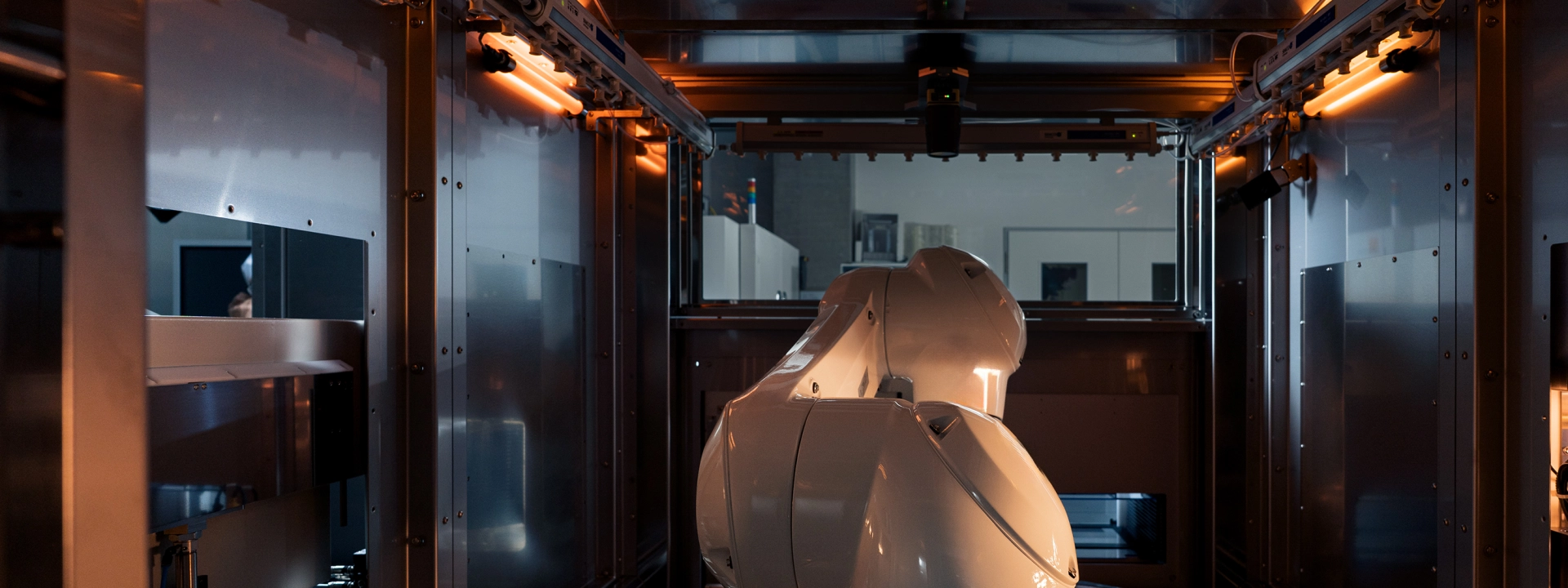
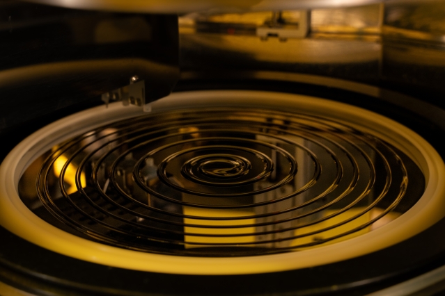
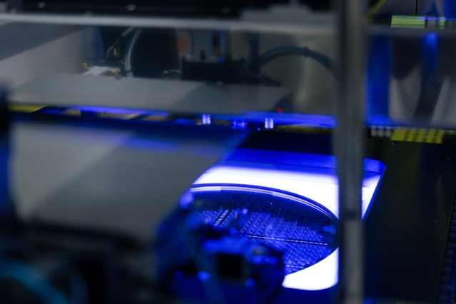
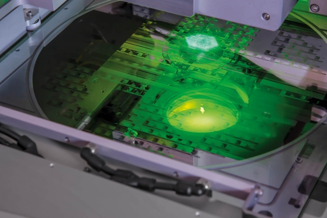
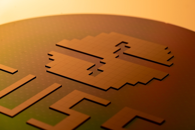
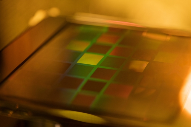
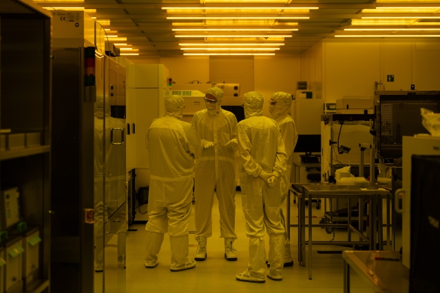
Process Technologies

In the quest for cost-effective manufacturing methods for powerful multifunction microchips, innovative process technologies have come to the fore in production planning. Carefully selecting suitable techniques allows greatly enhanced efficiency of production processes, increased yields and time savings throughout the entire manufacturing cycle. The systems offered by SUSS feature exceptional process flexibility, supporting numerous processes and easy setup modification.

Which are the right processes for manufacturing your products?

We are committed to providing competent advice and ensuring that, supported by our products, our customers are able to successfully compete in their markets. In order to meet the worldwide demand for process development support and feasibility studies, SUSS maintains regional application laboratories. Highly qualified process experts are available to support our customers with competence and experience for solving complex tasks.

Alignment

  • Top-side alignment (TSA)
  • Bottom-side alignment (BSA)
  • Infrared alignment (IR)

Top-side alignment (TSA)

Where lithographic processes require the alignment of structures on only one side of the device wafer (e.g. RDL, micro bumping, and similar techniques), top-side alignment is used to align the fiducials on the mask with those of the wafer. Depending on substrate properties, this can be achieved either using stored position data for the wafer or through live image alignment, as in the DirectAlign® system invented at SUSS.

Highlights

  • Mask aligner for the highest level of alignment precision
  • Clear and stable pattern recognition even under poor contrast conditions

Available for:

Manual Mask Aligner

Exposure

  • Proximity Lithography

A mask with a certain structure is aligned with the wafer in very close proximity (thus “proximity” lithography). During exposure, the shadow cast by the mask structure is transferred to the wafer. The resulting exposure quality depends on both the precision with which the mask and wafer are spaced apart and the optical system used for exposure.

Being fast and suited to flexible implementation, this method is regarded as the most cost-effective technique for producing microstructures down to 4 µm in size for 300 mm tools and down to 3.5 µm and 3 µm for 200 and 150 mm tools, respectively. With contact exposure, resolutions in the sub-micron range can be achieved. Typical areas of use include wafer-level chip-scale packaging, flip chip packaging, bumping, MEMS, LED, and power devices. The systems are deployed in high-volume production as well as in industrial research.

The mask aligners supplied by SUSS are based on proximity lithography.

Features & Benefits

  • Superior resolution as a result of diffraction-reducing optics
  • Process stability through the use of microlens optical systems

Available for:

Semi-Automated Mask Aligner
Manual Mask Aligner

Coating

  • Spin Coating
  • Spray Coating

Spin coating is the process of evenly coating a spinning substrate with a solution. The solution, for instance, a photosensitive resist, is dispensed at the center of the wafer. Subsequent acceleration as well as the rotation speed and the time allotted to the individual steps ensure that a homogeneous layer thickness remains after excess resist is spun off. Alongside the process parameters, the physical properties of the solution or photoresist determine the thickness of the applied film.

Spin coating is limited in use to structures without high topography.

Available for:

Semi-Automated Coaters and Developers
Manual Coater and Developer

Developing

  • Puddle Developing
  • Spray Developing

Puddle developing involves dispensing a defined quantity of developer to the exposed substrate, gently spinning it to spread the developer. Due to the surface tension of the developing agent, a convex puddle is formed on the wafer. Once developing time is completed, the wafer is rotated quickly to spin off the developer agent. The wafer is subsequently rinsed with deionized water and dried, once again at a high rotation speed. The main advantage of the technique is that only very little developing agent is required while maintaining excellent process results.

Puddle developing is no longer feasible when the developing agent becomes saturated, for example when a large quantity of photoresist needs to be removed or a high structural topography prevents exchange of the developer. In such cases, a multi-stage puddle developing process or spray developing is used.

Features and Benefits

  • Minimal chemical consumption

Available for:

Semi-Automated Coaters and Developers

Inkjet Printing

  • Inkjet Imprinting

Inkjet printing is an additive manufacturing technology applying functional materials for a variety of applications. These functional materials can have dielectric, conductive, adhesive, mechanical, optical or chemical properties, and are printed with pico-liter sized droplets from a digital file.

Its precise drop placement and accurate drop volumes make functional inkjet printing suited to printed electronics, displays, OLED, sensors, PCBs, semiconductor assembly, chemical machining, photovoltaics, life science and optics.

Inkjet printing can create fine features down to 20 microns, and replace techniques such as lithography, screen printing, spray coating and dispensing. There is no more need for masks and screens, significantly saving material usage and enabling short product changeover times.

With a typical distance between the substrate and the inkjet head of just under 1 mm, inkjet is a non-contact deposition technology. So, there is no risk of damaging fragile substrates. Inkjet can also deposit on top of existing 3D topology and fill trenches and cavities, which is a challenge for traditional techniques like screen printing.

Available for:

Bonding

  • Adhesive
  • Anodic
  • Eutectic
  • Glass Frit
  • Hybrid Bonding
  • Metal Diffusion
  • Slid
  • Fusion Bonding
  • Mechanical Debonding

Adhesive Bonding

A variety of materials are available for adhesive wafer bonding techniques utilizing polymers and adhesives, including epoxies, dry films, BCB, polyimides, and UV curable compounds.

Highlight:

  • Comparatively low temperature for protecting sensitive components

Available for:

Automated Bonder
Semi-Automated Bonder

Temporary Wafer Bonding

  • Temporary Wafer Bonding
  • Mechanical Debonding
  • Laser Debonding

To minimize the risks in thin wafer handling, the wafer is mounted on a carrier wafer prior to thinning. Bonding is only to facilitate further processing – the bond is designed to be dissolved once the wafer is processed.

Process steps required for temporary wafer bonding

  • Application of release layers (coating or plasma deposition)
  • Adhesive coating
  • Bonding
  • Thermal or UV curing

SUSS offers an open platform that is compatible with all common material systems used in temporary wafer bonding. In addition to the methods already used in production today, SUSS is devoted to ongoing work towards qualifying new materials, in this way supporting the largest selection of adhesives currently available in the market.

Highlights

  • Open bonding platform supporting flexible configuration and all common adhesives and techniques
  • Coating of bonding and release layers, including temporary bonding, in one system
  • Integrated metrology to determine wafer thickness and TTV

Available for:

Automated Temporary Bonder
Semi-Automated Bonder

Imprint Lithography

  • Imprint Lithography
  • SCIL
  • SMILE

Imprint lithography represents a cost-effective and highly reliable means of transferring three-dimensional nano- or micro-scale patterns onto a wide variety of substrates.

For the imprint, a stamp is brought into contact with a photosensitive material on the substrate. The photoresist fills out the three-dimensional pattern of the stamp and then solidifies under UV light. Parameters such as pattern topography, structure resolution and aspect ratio have a considerable influence on the process quality.
Thanks to its compatibility with well-established semiconductor processes, imprint lithography plays a key role in the development and production of devices in the field of LED, MEMS/NEMS, micro-optics, augmented reality and opto-electronic sensors using the renowned SMILE technology.

SUSS solutions for imprint lithography are based on manual mask aligner platforms and support a wide range of materials and substrate with sizes up to 200 mm. Furthermore, SUSS platforms provide the capability to align and level stamps to substrates, as required by many imprint applications. Imprint equipment can also be retrofitted to SUSS mask aligners which are already in the field.

インプリントリソグラフィのWebページ

インプリントリソグラフィのパンフレット

Available for:

Manual Mask Aligner

Plasma Activation

  • Plasma Activation
  • Wafer Preparation for Fusion Bonding

Plasma treatments alter the properties of the substrate surface and are used for wafer and direct bonding applications. To achieve uniform plasma discharge, two electrodes are required, at least one of which has to have a sufficiently thick dielectric layer, and the intermediate gap has to be sufficiently small. When alternating voltage is applied, a uniform discharge ensues even under atmospheric pressure, making the use of costly vacuum technology obsolete.

Photomask Cleaning

  • Photomask Cleaning
  • Surface Preparation
  • Surface Purification and Preservation
  • Wet Cleaning

Contamination of the mask affects the correct imaging process in the lithography tool during device manufacturing. Sub-micron particles as well as organic and inorganic contamination threaten to endanger yield. Thus, preparation, cleaning and handling of photomasks are playing a vital part in lithographical production processes. Moreover, next-generation lithography with its drive to go to technology nodes down to 22nm hp and beyond requires very efficient cleaning technologies by avoiding pattern damage and changes in optical properties as much as possible. A “zero particles” philosophy is therefore indispensable.

Substrates range from conventional binary photomasks of all kind of materials to phase-shift masks (PSM). Each requires matching techniques regarding cleaning in the photomask production process as well as during application by the end users (device manufacturers).

A comprehensive cleaning process involves:

  • Surface preparation
  • Resist strip and organic removal
  • Particle removal
  • Residual ion removal
  • Drying, surface purification and preservation