Projection Scanner

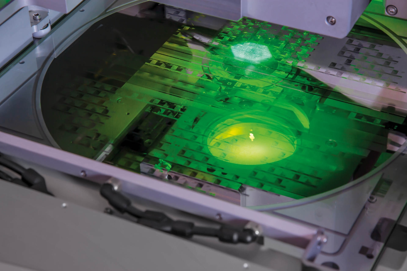
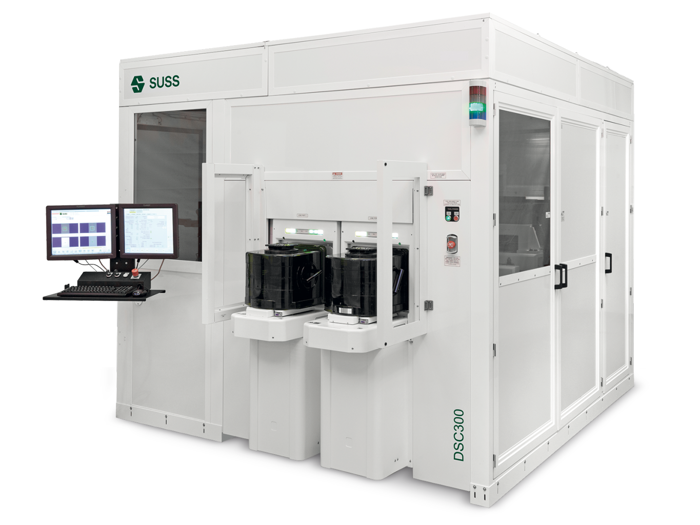
Noted for its highly accurate alignment and precise exposure optics, SUSS’s product portfolio of proximity printing equipment is complemented by a unique projection lithography solution. The projection scanner platform DSC combines the advantages of full-field lithography with the imaging performance of projection lithography, offering a very cost-efficient alternative to projection steppers. Equipped with a full-field mask and broadband projection optics, the system exposes the substrate in a single continuous scanning mode.

The projection scanner platform is suited for applications such as advanced packaging, especially wafer-level chip-scale packaging and flip-chip packaging, 3D integration, MEMS and displays.

Technologies

  • Projection Lithography

Projection exposure entails aligning the mask with the wafer. The mask pattern is subsequently projected onto the wafer by means of an optical system between the mask and the wafer. With this process, usually only a portion of the wafer is exposed. By repeating the process incrementally ("step and repeat") or through a continuous process ("scanning"), the wafer is completely exposed. The type and the characteristics of the projection optics are decisive factors for resolution and depth of focus and thus for the effectiveness of the exposure.

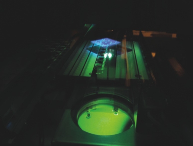
The projection scanner technology offered by SUSS utilizes the combined advantages of full-field exposure and conventional projection lithography, and serves as an alternative to mask aligners and conventional projection steppers. Projection scanning involves aligning a full-field mask with the substrate and then projecting the mask pattern onto the substrate by means of scanning. Scanning technology achieves greater throughput than stepper processes, while at the same time reducing system costs and achieving resolutions down to 3 µm.

Projection scanning offers the greatest advantage in processes requiring high resolutions or where high topography and thick resist coatings are involved.

Features & Benefits

  • Cost-effective projection solution offering superior resolution down to 3 µm
  • Steep resist sidewalls in thick resist processes

Available for: